- 您现在的位置:买卖IC网 > Sheet目录17367 > ISL85033EVAL2Z (Intersil)EVAL BOARD2 FOR ISL85033
�� �
�
�ISL85033�
�Vo�
�Put� the� compensator� zero� at� 6.6kHz� (~1.5x� C� o� R� o� ),� and� put� the�
�compensator� pole� at� ESR� zero,� which� is� 1.45MHz.� The�
�R� 2�
�R� 3�
�C� 3�
�V� FB�
�V� REF�
�-�
�+�
�GM�
�V� COMP�
�R� 1�
�C� 2�
�compensator� capacitors� are:�
�C� 1� =� 470pF,� C� 2� =� 3pF� (There� is� approximately� 3pF� parasitic�
�capacitance� from� V� COMP� to� GND;� therefore,� C� 2� is� optional).�
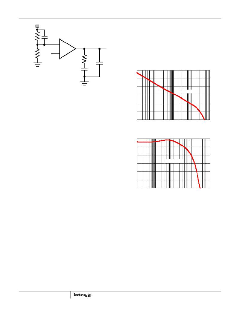
�Figure� 48A� shows� the� simulated� voltage� loop� gain.� It� is� shown�
�that� it� has� 80kHz� loop� bandwidth� with� 69°� phase� margin� and�
�15dB� gain� margin.� Optional� addition� phase� boost� can� be� added�
�to� the� overall� loop� response� by� using� C� 3� .�
�C� 1�
�60�
�45�
�FIGURE� 47.� TYPE� II� COMPENSATOR�
�Figure� 47� shows� the� type� II� compensator� and� its� transfer� function�
�is� expressed� as� Equation� 23:�
�30�
�15�
�GAIN� (dB)�
�?� 1� +� ------------� ?� ?� 1� +� ------------� ?�
�ω� cz1�
�ω� cz2�
�g� m�
�v� ?� comp�
�A� v� (� S� )� =� ----------------� =� -------------------� ---------------------------------------------------------�
�C� 1� +� C� 2�
�v� ?� FB�
�S� 1� +� ----------� ?�
�?� ω� ?�
�Where:�
�S� S�
�?� ?� ?� ?�
�?� S�
�cp�
�(EQ.� 23)�
�0�
�-15�
�-30�
�100�
�1?10� 3�
�1?10� 4�
�FIGURE� 48A.�
�1?10� 5�
�1?10� 6�
�ω� cz1� =� --------------� ,� ω� cz2� =� --------------� ,� ω� cp� =� ---------------------�
�R� 1� C� 1� R� 2� C� 3� R� 1� C� 1� C� 2�
�the� compensator� design� goal� is:�
�High� DC� gain�
�1� 1� C� 1� +� C� 2�
�(EQ.� 24)�
�100�
�80�
�Loop� bandwidth� f� c� :� ?� --� 4� -� to� -------� ?� f� s�
�Gain� margin:� >10dB�
�Phase� margin:� 40°�
�?� 1� 1� ?�
�10�
�60�
�40�
�20�
�PHASE (°)�
�(EQ.� 25)�
�Put� compensator� zero� ω� cz1� =� (� 1to3� )� ---------------�
�R� C�
�The� compensator� design� procedure� is� shown� in� Equation� 25:�
�1�
�O� O�
�Put� one� compensator� pole� at� zero� frequency� to� achieve� high� DC�
�0�
�-20�
�100�
�1?10� 3�
�1?10� 4�
�1?10� 5�
�1?10� 6�
�2� π� f� c� V� o� C� o� R� T�
�R� 1� =� ---------------------------------�
�(EQ.� 27)�
�C� 1� =� -----------------� ,� C� 2� =� -------------------------�
�P� D� [� W� ]� =� I� OUT� ?� V� D� ?� ?� ?�
�?� V� OUT� ?� (EQ.� 28)�
�V� IN� ?�
�gain,� and� put� another� compensator� pole� at� either� ESR� zero�
�frequency� or� half� switching� frequency,� whichever� is� lower.�
�The� loop� gain� T� v� (S)� at� crossover� frequency� of� f� c� has� unity� gain.�
�Therefore,� the� compensator� resistance� R� 1� is� determined� by�
�Equation� 26:�
�(EQ.� 26)�
�g� m� V� FB�
�where� g� m� is� the� trans-conductance� of� the� voltage� error� amplifier,�
�typically� 200μA/V.� Compensator� capacitor� C� 1� is� then� given� by�
�Equation� 27:�
�1� 1�
�R� 1� ω� cz� 2� π� R� 1� f� esr�
�Example:� V� IN� =� 12V,� V� o� =� 5V,� I� o� =� 3A,� f� s� =� 500kHz,�
�C� o� =� 220μF/5m� Ω� ,� L� =� 5.6μH,� g� m� =� 200μs,� R� T� =� 0.21,�
�V� FB� =� 0.8V,� S� e� =� 1.1� � 10� 5� V/s,� S� n� =� 3.4� � 10� 5� V/s,� f� c� =� 80kHz,� then�
�compensator� resistance� R� 1� =� 72k� Ω� .�
�21�
�FIGURE� 48B.�
�Rectifier� Selection�
�Current� circulates� from� ground� to� the� junction� of� the� external�
�Schottky� diode� and� the� inductor� when� the� high-side� switch� is� off.�
�As� a� consequence,� the� polarity� of� the� switching� node� is� negative�
�with� respect� to� ground.� This� voltage� is� approximately� -0.5V� (a�
�Schottky� diode� drop)� during� the� off-time.� The� rectifier's� rated�
�reverse� breakdown� voltage� must� be� at� least� equal� to� the�
�maximum� input� voltage,� preferably� with� a� 20%� derating� factor.�
�The� power� dissipation� when� the� Schottky� diode� conducts� is�
�expressed� in� Equation� 28:�
�1� –� -------------�
�?�
�Where:�
�V� D� is� the� voltage� drop� of� the� Schottky� diode.� Selection� of� the�
�Schottky� diode� is� critical� in� terms� of� the� high� temperature�
�reverse� bias� leakage� current� which� is� very� dependent� on� VIN� and�
�FN6676.6�
�February� 23,� 2012�
�发布紧急采购,3分钟左右您将得到回复。
相关PDF资料
MIC5891BWM
IC DRVR LATCH 8BIT SER IN 16SOIC
MIC5891BN
IC DRVR LATCH 8BIT SER IN 16DIP
TAAB336K010G
CAP TANT 33UF 10V 10% AXIAL
SPX385AS-L-1-2
IC VREF SHUNT PREC 1.235V 8SOICN
A9AAT-1105F
FLEX CABLE - AFE11T/AF11/AFE11T
TDC225K025NSE
CAP TANT 2.2UF 25V 10% RADIAL
MIC5841BWM TR
IC DRVR LATCH 8BIT SER IN 18SOIC
SPX432AM-L
IC VREF SHUNT PREC ADJ SOT-23-3
相关代理商/技术参数
ISL85033IRTZ
功能描述:IC REG BUCK SYNC ADJ 3A 28TQFN RoHS:是 类别:集成电路 (IC) >> PMIC - 稳压器 - DC DC 开关稳压器 系列:- 产品培训模块:Lead (SnPb) Finish for COTS
Obsolescence Mitigation Program 标准包装:2,500 系列:- 类型:降压(降压) 输出类型:两者兼有 输出数:1 输出电压:5V,1 V ~ 10 V 输入电压:3.5 V ~ 28 V PWM 型:电流模式 频率 - 开关:220kHz ~ 1MHz 电流 - 输出:600mA 同步整流器:无 工作温度:-40°C ~ 125°C 安装类型:表面贴装 封装/外壳:16-SSOP(0.154",3.90mm 宽) 包装:带卷 (TR) 供应商设备封装:16-QSOP
ISL85033IRTZ-T
功能描述:IC REG BUCK SYNC ADJ 3A 28TQFN RoHS:是 类别:集成电路 (IC) >> PMIC - 稳压器 - DC DC 开关稳压器 系列:- 产品培训模块:Lead (SnPb) Finish for COTS
Obsolescence Mitigation Program 标准包装:2,500 系列:- 类型:降压(降压) 输出类型:两者兼有 输出数:1 输出电压:5V,1 V ~ 10 V 输入电压:3.5 V ~ 28 V PWM 型:电流模式 频率 - 开关:220kHz ~ 1MHz 电流 - 输出:600mA 同步整流器:无 工作温度:-40°C ~ 125°C 安装类型:表面贴装 封装/外壳:16-SSOP(0.154",3.90mm 宽) 包装:带卷 (TR) 供应商设备封装:16-QSOP
ISL85033IRTZ-T7A
功能描述:直流/直流开关调节器 3A STD BUCK REG - 4X 4 TQFN 250 PC REEL RoHS:否 制造商:International Rectifier 最大输入电压:21 V 开关频率:1.5 MHz 输出电压:0.5 V to 0.86 V 输出电流:4 A 输出端数量: 最大工作温度: 安装风格:SMD/SMT 封装 / 箱体:PQFN 4 x 5
ISL8505IRZ
制造商:Intersil Corporation 功能描述:PB-FREE DC TO DC POWER SWITCHING, 38LD QFN 5X7 - Rail/Tube
ISL8510EVAL1Z
功能描述:EVALUATION BOARD FOR ISL8510 RoHS:是 类别:编程器,开发系统 >> 评估板 - DC/DC 与 AC/DC(离线)SMPS 系列:- 产品培训模块:Obsolescence Mitigation Program 标准包装:1 系列:True Shutdown™ 主要目的:DC/DC,步升 输出及类型:1,非隔离 功率 - 输出:- 输出电压:- 电流 - 输出:1A 输入电压:2.5 V ~ 5.5 V 稳压器拓扑结构:升压 频率 - 开关:3MHz 板类型:完全填充 已供物品:板 已用 IC / 零件:MAX8969
ISL8510IRZ
功能描述:IC REG DL BUCK/LINEAR 24-QFN RoHS:是 类别:集成电路 (IC) >> PMIC - 稳压器 - 线性 + 切换式 系列:- 标准包装:2,500 系列:- 拓扑:降压(降压)同步(3),线性(LDO)(2) 功能:任何功能 输出数:5 频率 - 开关:300kHz 电压/电流 - 输出 1:控制器 电压/电流 - 输出 2:控制器 电压/电流 - 输出 3:控制器 带 LED 驱动器:无 带监控器:无 带序列发生器:是 电源电压:5.6 V ~ 24 V 工作温度:-40°C ~ 85°C 安装类型:* 封装/外壳:* 供应商设备封装:* 包装:*
ISL8510IRZ-T
功能描述:IC REG DL BUCK/LINEAR 24-QFN RoHS:是 类别:集成电路 (IC) >> PMIC - 稳压器 - 线性 + 切换式 系列:- 标准包装:2,500 系列:- 拓扑:降压(降压)同步(3),线性(LDO)(2) 功能:任何功能 输出数:5 频率 - 开关:300kHz 电压/电流 - 输出 1:控制器 电压/电流 - 输出 2:控制器 电压/电流 - 输出 3:控制器 带 LED 驱动器:无 带监控器:无 带序列发生器:是 电源电压:5.6 V ~ 24 V 工作温度:-40°C ~ 85°C 安装类型:* 封装/外壳:* 供应商设备封装:* 包装:*
ISL85402EVAL1Z
制造商:Intersil Corporation 功能描述:ISL85402 EVAL BOARD1 - 20LD QFN - INPUT VOLTAGE 36V, 2.5A - Bulk